

Подробную информацию о продукте см. в характеристиках.
TLC320AD77CDB
Product Overview
Category
The TLC320AD77CDB belongs to the category of analog-to-digital converters (ADCs).
Use
This product is primarily used for converting analog signals into digital data, making it suitable for various applications in industries such as telecommunications, audio processing, and instrumentation.
Characteristics
- High-resolution: The TLC320AD77CDB offers a high resolution of [specify resolution].
- Low power consumption: It operates on low power, making it energy-efficient.
- Fast conversion rate: The ADC provides a fast conversion rate of [specify rate].
- Wide input voltage range: It can handle a wide range of input voltages, allowing for versatile usage.
- Noise reduction: The device incorporates noise reduction techniques to ensure accurate signal conversion.
Package and Quantity
The TLC320AD77CDB is available in a [specify package type] package. Each package contains [specify quantity] units of the product.
Specifications
- Resolution: [specify resolution]
- Input Voltage Range: [specify range]
- Conversion Rate: [specify rate]
- Power Supply: [specify supply voltage]
- Operating Temperature Range: [specify temperature range]
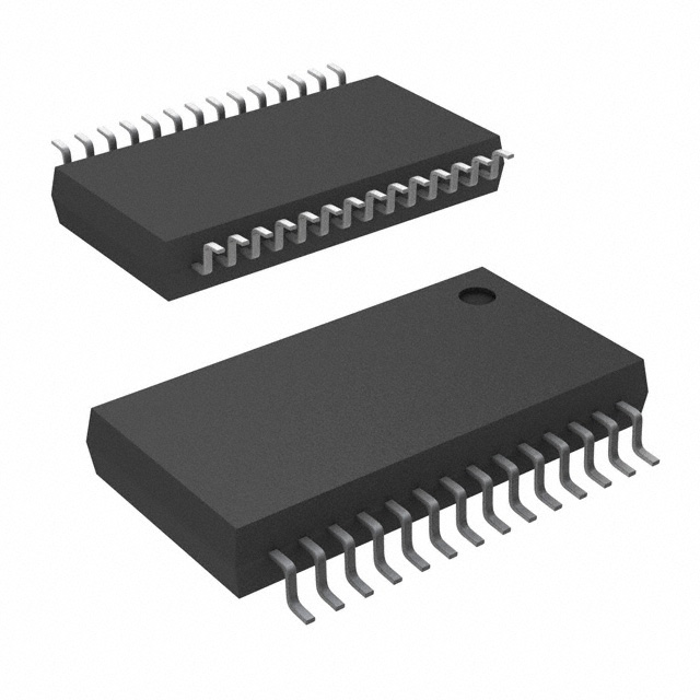
Pin Configuration
The TLC320AD77CDB has [specify number of pins] pins arranged as follows:
- Pin 1: [specify pin function]
- Pin 2: [specify pin function]
- Pin 3: [specify pin function] ... ...
Functional Features
- High precision: The TLC320AD77CDB ensures accurate and precise conversion of analog signals.
- Versatile input options: It supports multiple input configurations, including single-ended and differential inputs.
- Digital interface: The ADC features a digital interface for easy integration with microcontrollers or other digital systems.
- Programmable gain: Users can adjust the gain of the ADC to suit their specific application requirements.
- Low distortion: The device minimizes distortion during signal conversion, resulting in high-quality digital data.
Advantages and Disadvantages
Advantages
- High resolution and accuracy
- Low power consumption
- Versatile input options
- Programmable gain for flexibility
- Low distortion for high-quality output
Disadvantages
- [Specify any disadvantages or limitations]
Working Principles
The TLC320AD77CDB operates based on the principle of analog-to-digital conversion. It takes an analog input signal and converts it into a corresponding digital representation using internal circuitry and algorithms. The ADC samples the analog signal at a specified rate, quantizes it into discrete levels, and outputs the digital data.
Application Field Plans
The TLC320AD77CDB finds applications in various fields, including: 1. Telecommunications: Used in voice communication systems, teleconferencing equipment, etc. 2. Audio processing: Integrated into audio recording devices, mixers, and amplifiers. 3. Instrumentation: Utilized in measurement and control systems, data acquisition devices, etc.
Alternative Models
For users seeking alternative options, the following models are worth considering: 1. Model 1: [Provide details of the alternative model] 2. Model 2: [Provide details of the alternative model] 3. Model 3: [Provide details of the alternative model]
Please note that the specifications and features of alternative models may vary.
Перечислите 10 распространенных вопросов и ответов, связанных с применением TLC320AD77CDB в технических решениях.
Sure! Here are 10 common questions and answers related to the application of TLC320AD77CDB in technical solutions:
Question: What is TLC320AD77CDB?
- Answer: TLC320AD77CDB is a high-performance, 24-bit analog-to-digital converter (ADC) designed for use in various technical applications.Question: What is the resolution of TLC320AD77CDB?
- Answer: The TLC320AD77CDB has a resolution of 24 bits, allowing for precise and accurate conversion of analog signals into digital data.Question: What is the sampling rate of TLC320AD77CDB?
- Answer: The TLC320AD77CDB supports a maximum sampling rate of 192 kHz, enabling fast and real-time conversion of analog signals.Question: What is the input voltage range of TLC320AD77CDB?
- Answer: The TLC320AD77CDB has a differential input voltage range of ±2.5V, making it suitable for a wide range of signal levels.Question: Does TLC320AD77CDB require an external reference voltage?
- Answer: Yes, TLC320AD77CDB requires an external reference voltage for accurate conversion. It supports both single-ended and differential reference inputs.Question: What interfaces does TLC320AD77CDB support?
- Answer: TLC320AD77CDB supports serial interfaces such as I2C and SPI, allowing for easy integration with microcontrollers and other digital devices.Question: Can TLC320AD77CDB operate in low-power mode?
- Answer: Yes, TLC320AD77CDB features a low-power mode that reduces power consumption during idle or standby periods, making it energy-efficient.Question: What is the operating temperature range of TLC320AD77CDB?
- Answer: The TLC320AD77CDB can operate within a temperature range of -40°C to +85°C, making it suitable for various environmental conditions.Question: Does TLC320AD77CDB provide any built-in digital filters?
- Answer: Yes, TLC320AD77CDB includes programmable digital filters that can be used to enhance the quality and accuracy of the converted digital data.Question: Are there any evaluation boards or development kits available for TLC320AD77CDB?
- Answer: Yes, Texas Instruments provides evaluation boards and development kits for TLC320AD77CDB, which can help in the prototyping and testing of applications using this ADC.
Please note that these questions and answers are general and may vary depending on specific application requirements and use cases.