

Подробную информацию о продукте см. в характеристиках.
XC2VP70-5FFG1517C
Product Overview
Category
XC2VP70-5FFG1517C belongs to the category of Field Programmable Gate Arrays (FPGAs).
Use
This FPGA is designed for various applications that require high-performance digital signal processing, such as telecommunications, video processing, and image recognition.
Characteristics
- High-speed processing capabilities
- Configurable logic blocks
- On-chip memory resources
- Flexible I/O interfaces
- Low power consumption
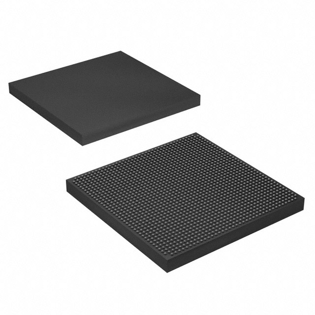
Package
XC2VP70-5FFG1517C is available in a Flip Chip FineLine BGA package.
Essence
The essence of XC2VP70-5FFG1517C lies in its ability to provide reconfigurable hardware that can be customized for specific applications, offering flexibility and performance advantages over traditional fixed-function integrated circuits.
Packaging/Quantity
XC2VP70-5FFG1517C is typically sold individually or in small quantities, depending on the supplier.
Specifications
- Device Type: FPGA
- Family: Virtex-II Pro
- Logic Cells: 70,000
- System Gates: 1.5 million
- RAM Blocks: 864
- Maximum Frequency: 500 MHz
- Operating Voltage: 1.8V
- Package Type: Flip Chip FineLine BGA
- Package Pins: 1517
- Temperature Range: -40°C to +100°C
Detailed Pin Configuration
The detailed pin configuration of XC2VP70-5FFG1517C can be found in the manufacturer's datasheet. It provides information about the specific functions and connections of each pin on the FPGA.
Functional Features
XC2VP70-5FFG1517C offers several functional features that make it suitable for demanding applications:
High-Speed Processing: The FPGA's architecture allows for efficient parallel processing, enabling high-speed data manipulation and computation.
Configurable Logic Blocks: The device contains numerous configurable logic blocks that can be programmed to implement various digital functions.
On-Chip Memory Resources: XC2VP70-5FFG1517C includes embedded memory blocks, which can be used for storing data or implementing complex algorithms.
Flexible I/O Interfaces: The FPGA supports a wide range of input/output standards, allowing seamless integration with external devices.
Low Power Consumption: Despite its high-performance capabilities, XC2VP70-5FFG1517C is designed to minimize power consumption, making it suitable for battery-powered applications.
Advantages and Disadvantages
Advantages
- High-performance processing capabilities
- Flexibility to adapt to changing requirements
- Efficient utilization of hardware resources
- Support for various communication protocols
- Low power consumption compared to alternative solutions
Disadvantages
- Higher cost compared to fixed-function integrated circuits
- Steeper learning curve for programming and configuration
- Limited availability of technical support for specific applications
Working Principles
XC2VP70-5FFG1517C operates based on the principles of reconfigurable computing. It consists of an array of configurable logic blocks interconnected through programmable routing resources. These logic blocks can be programmed to implement desired digital functions, allowing the FPGA to perform specific tasks according to the user's requirements.
Detailed Application Field Plans
XC2VP70-5FFG1517C finds applications in various fields, including:
Telecommunications: The FPGA can be used for signal processing in wireless communication systems, such as baseband processing, channel coding, and modulation/demodulation.
Video Processing: XC2VP70-5FFG1517C enables real-time video processing tasks, such as video compression, image enhancement, and object recognition.
Image Recognition: The FPGA's high-speed processing capabilities make it suitable for image recognition applications, including facial recognition, object detection, and pattern matching.
Industrial Automation: XC2VP70-5FFG1517C can be utilized in industrial automation systems for tasks like control logic implementation, sensor interfacing, and data acquisition.
Detailed and Complete Alternative Models
XC2VP100-6FF1704C: This FPGA offers higher logic capacity and system gates compared to XC2VP70-5FFG1517C, making it suitable for more complex applications.
XC2V2000-4FF896C: With significantly larger logic cells and memory resources, this FPGA provides enhanced performance for demanding digital signal processing tasks.
XC2S50-5TQ144C: This smaller FPGA is suitable for low-cost applications that require moderate processing capabilities and I/O interfaces.
XC2C256-7TQ144C: Designed for small-scale projects, this FPGA offers a cost-effective solution with limited logic capacity and I/O options.
These alternative models provide varying levels of performance
Перечислите 10 распространенных вопросов и ответов, связанных с применением XC2VP70-5FFG1517C в технических решениях.
Sure! Here are 10 common questions and answers related to the application of XC2VP70-5FFG1517C in technical solutions:
Q: What is XC2VP70-5FFG1517C? A: XC2VP70-5FFG1517C is a field-programmable gate array (FPGA) manufactured by Xilinx. It offers high-performance computing capabilities and is commonly used in various technical solutions.
Q: What are the key features of XC2VP70-5FFG1517C? A: Some key features of XC2VP70-5FFG1517C include a large number of logic cells, high-speed I/O interfaces, embedded memory blocks, and support for various communication protocols.
Q: In what applications can XC2VP70-5FFG1517C be used? A: XC2VP70-5FFG1517C can be used in a wide range of applications such as telecommunications, aerospace, defense, industrial automation, medical devices, and scientific research.
Q: How does XC2VP70-5FFG1517C enhance system performance? A: XC2VP70-5FFG1517C enhances system performance by providing parallel processing capabilities, hardware acceleration, and real-time data processing, which can significantly improve overall system speed and efficiency.
Q: Can XC2VP70-5FFG1517C be reprogrammed after deployment? A: Yes, XC2VP70-5FFG1517C is a field-programmable device, meaning it can be reprogrammed even after it has been deployed in a system. This flexibility allows for easy updates and modifications.
Q: What development tools are available for programming XC2VP70-5FFG1517C? A: Xilinx provides various development tools such as Vivado Design Suite and ISE Design Suite, which offer comprehensive features for designing, simulating, and programming XC2VP70-5FFG1517C.
Q: Can XC2VP70-5FFG1517C interface with other components or devices? A: Yes, XC2VP70-5FFG1517C supports a wide range of interfaces including PCIe, Ethernet, USB, SPI, I2C, and more, allowing it to easily communicate and interface with other components or devices.
Q: What are the power requirements for XC2VP70-5FFG1517C? A: XC2VP70-5FFG1517C typically requires a supply voltage of 1.2V and auxiliary voltages for different I/O standards. The specific power requirements can be found in the device datasheet.
Q: Are there any temperature limitations for XC2VP70-5FFG1517C? A: Yes, XC2VP70-5FFG1517C has specified operating temperature ranges. It is important to ensure that the device operates within these temperature limits to maintain reliable performance.
Q: Where can I find additional resources and support for XC2VP70-5FFG1517C? A: Xilinx provides comprehensive documentation, application notes, reference designs, and technical support through their website and community forums. Additionally, authorized distributors may also offer assistance and resources.