

Подробную информацию о продукте см. в характеристиках.
XC4005XL-2PC84I
Product Overview
Category
XC4005XL-2PC84I belongs to the category of programmable logic devices (PLDs).
Use
This product is commonly used in digital circuit design and implementation. It provides a flexible and customizable solution for various applications.
Characteristics
- Programmable: The XC4005XL-2PC84I can be programmed to perform specific functions according to the user's requirements.
- High-density: It offers a high number of logic elements, allowing for complex designs.
- Low power consumption: The device is designed to operate efficiently with minimal power consumption.
- Fast operation: The XC4005XL-2PC84I has a high-speed performance, enabling quick execution of logic operations.
Package
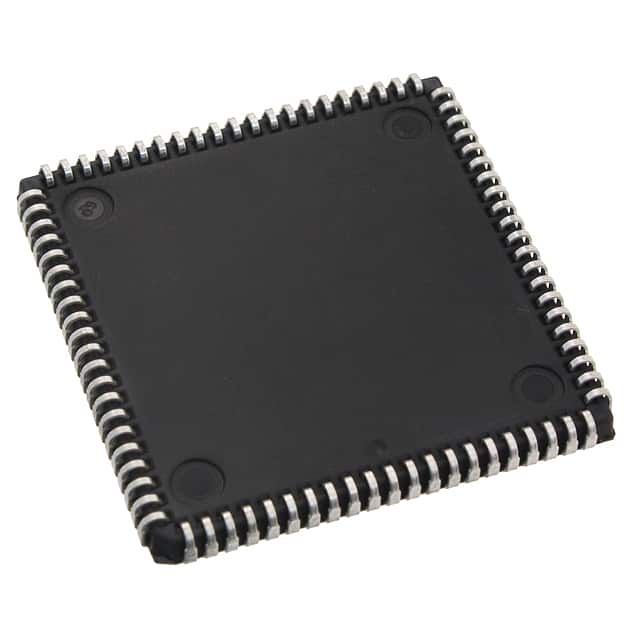
The XC4005XL-2PC84I comes in a 84-pin plastic quad flat pack (PQFP) package.
Essence
The essence of XC4005XL-2PC84I lies in its ability to provide reconfigurable logic functionality, allowing users to implement custom digital circuits without the need for dedicated hardware.
Packaging/Quantity
The XC4005XL-2PC84I is typically packaged individually and is available in various quantities depending on the supplier.
Specifications
- Logic Elements: 4000
- Flip-Flops: 128
- Maximum Frequency: 100 MHz
- Operating Voltage: 3.3V
- I/O Pins: 68
- Maximum User I/Os: 64
- JTAG Pins: 4
- Configuration Bits: 5000
- Operating Temperature Range: -40°C to 85°C
Detailed Pin Configuration
The XC4005XL-2PC84I has a total of 84 pins. Here is a brief overview of some important pin groups:
Power Supply:
- VCCINT: Internal power supply (3.3V)
- VCCIO: I/O power supply (3.3V)
Configuration:
- TDI: Test Data Input
- TDO: Test Data Output
- TCK: Test Clock
- TMS: Test Mode Select
I/O Pins:
- IO0 to IO67: General-purpose I/O pins
- GND: Ground pin
Other Pins:
- CCLK: Configuration Clock
- DONE: Configuration Done
- INIT: Initialization
For a complete pin configuration, please refer to the XC4005XL-2PC84I datasheet.
Functional Features
The XC4005XL-2PC84I offers several functional features that make it a versatile programmable logic device:
- Look-Up Tables (LUTs): The device contains a large number of LUTs that can be programmed to implement various logic functions.
- Flip-Flops: It includes a significant number of flip-flops for storing and synchronizing data.
- Programmable Interconnect: The XC4005XL-2PC84I allows users to configure the interconnections between logic elements, enabling complex circuit designs.
- Dedicated Function Blocks: The device incorporates dedicated blocks for specific functions such as arithmetic operations, memory, and clock management.
Advantages and Disadvantages
Advantages
- Flexibility: The XC4005XL-2PC84I provides the flexibility to create custom digital circuits without the need for dedicated hardware.
- High-density: With a large number of logic elements, it can handle complex designs.
- Low power consumption: The device operates efficiently with minimal power requirements.
- Fast operation: It offers high-speed performance for quick execution of logic operations.
Disadvantages
- Limited I/O Pins: The XC4005XL-2PC84I has a limited number of I/O pins, which may restrict the connectivity options for certain applications.
- Configuration Time: The device requires configuration before use, which can add complexity and time to the design process.
Working Principles
The XC4005XL-2PC84I operates based on the principles of programmable logic. It consists of configurable logic elements, interconnects, and dedicated function blocks. The user programs the device using a hardware description language (HDL) or a schematic entry tool. The programmed configuration is then loaded into the device, enabling it to perform the desired logic functions.
Detailed Application Field Plans
The XC4005XL-2PC84I finds applications in various fields, including:
- Embedded Systems: It can be used in the development of embedded systems, providing customizable logic functionality for specific requirements.
- Communication Systems: The device can be utilized in communication systems for protocol handling, data processing, and signal routing.
- Industrial Automation: It finds application in industrial automation systems for control and monitoring tasks.
- Consumer Electronics: The XC4005XL-2PC84I can be integrated into consumer electronic
Перечислите 10 распространенных вопросов и ответов, связанных с применением XC4005XL-2PC84I в технических решениях.
Sure! Here are 10 common questions and answers related to the application of XC4005XL-2PC84I in technical solutions:
Q: What is XC4005XL-2PC84I? A: XC4005XL-2PC84I is a field-programmable gate array (FPGA) manufactured by Xilinx.
Q: What are the key features of XC4005XL-2PC84I? A: Some key features of XC4005XL-2PC84I include 4000 logic cells, 64 macrocells, 32 I/O pins, and a maximum operating frequency of 100 MHz.
Q: What are the typical applications of XC4005XL-2PC84I? A: XC4005XL-2PC84I is commonly used in various digital design applications such as telecommunications, industrial control systems, automotive electronics, and consumer electronics.
Q: How can I program XC4005XL-2PC84I? A: XC4005XL-2PC84I can be programmed using Xilinx's Integrated Software Environment (ISE) or other compatible programming tools.
Q: Can XC4005XL-2PC84I be reprogrammed after it has been programmed once? A: Yes, XC4005XL-2PC84I is a reprogrammable FPGA, which means it can be reprogrammed multiple times.
Q: What is the power supply requirement for XC4005XL-2PC84I? A: XC4005XL-2PC84I typically operates on a 3.3V power supply.
Q: Does XC4005XL-2PC84I support external memory interfaces? A: Yes, XC4005XL-2PC84I supports various external memory interfaces such as SDRAM, SRAM, and Flash.
Q: Can XC4005XL-2PC84I interface with other digital components or microcontrollers? A: Yes, XC4005XL-2PC84I can interface with other digital components or microcontrollers through its I/O pins.
Q: What is the maximum operating temperature range for XC4005XL-2PC84I? A: XC4005XL-2PC84I has a maximum operating temperature range of -40°C to 100°C.
Q: Are there any development boards or evaluation kits available for XC4005XL-2PC84I? A: Yes, Xilinx offers development boards and evaluation kits specifically designed for XC4005XL-2PC84I, which can help in prototyping and testing applications.
Please note that these answers are general and may vary depending on specific requirements and application scenarios.