

Подробную информацию о продукте см. в характеристиках.
XC4006E-2PC84C
Product Overview
Category
XC4006E-2PC84C belongs to the category of Field Programmable Gate Arrays (FPGAs).
Use
This product is primarily used in digital circuit design and implementation. FPGAs provide a flexible and customizable solution for various applications, including telecommunications, automotive, aerospace, and consumer electronics.
Characteristics
- High integration: XC4006E-2PC84C offers a large number of logic elements, allowing complex designs to be implemented on a single chip.
- Reconfigurability: FPGAs can be reprogrammed multiple times, enabling rapid prototyping and design iterations.
- Parallel processing: The parallel architecture of FPGAs allows for efficient execution of multiple tasks simultaneously.
- Low power consumption: XC4006E-2PC84C is designed to minimize power consumption, making it suitable for battery-powered devices.
- High performance: FPGAs offer high-speed operation and can handle complex computations efficiently.
Package and Quantity
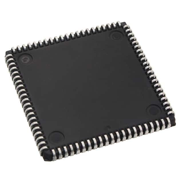
XC4006E-2PC84C is available in a 84-pin plastic quad flat pack (PQFP) package. It is typically sold in quantities of one unit per package.
Specifications
- Logic Elements: XC4006E-2PC84C provides 4000 usable gates or equivalent logic elements.
- I/O Pins: It offers 68 input/output pins for interfacing with external devices.
- Clock Management: The FPGA includes built-in clock management resources, such as phase-locked loops (PLLs) for generating stable clock signals.
- Memory: XC4006E-2PC84C features embedded memory blocks for storing data.
- Operating Voltage: The recommended operating voltage range is 3.3V to 5V.
Pin Configuration
The detailed pin configuration of XC4006E-2PC84C can be found in the product datasheet.
Functional Features
- Programmability: XC4006E-2PC84C can be programmed using Hardware Description Languages (HDLs) like VHDL or Verilog.
- Configurable Logic Blocks (CLBs): The FPGA contains CLBs that can be configured to implement various logic functions.
- Routing Resources: XC4006E-2PC84C provides a network of programmable interconnects, allowing signals to be routed between different logic elements.
- I/O Interfaces: The FPGA supports various I/O standards, such as LVCMOS, LVTTL, and LVDS, enabling easy integration with external devices.
Advantages and Disadvantages
Advantages
- Flexibility: FPGAs offer the ability to create custom digital circuits tailored to specific requirements.
- Time-to-Market: With FPGAs, designers can quickly prototype and iterate their designs, reducing time-to-market.
- Cost-effective: FPGAs eliminate the need for custom ASIC development, making them a cost-effective solution for low to medium volume production.
Disadvantages
- Power Consumption: Compared to dedicated application-specific integrated circuits (ASICs), FPGAs generally consume more power.
- Complexity: Designing for FPGAs requires expertise in hardware description languages and understanding of FPGA architecture.
- Limited Performance: While FPGAs offer high performance, they may not match the speed of specialized ASICs for certain applications.
Working Principles
XC4006E-2PC84C operates based on the principles of reconfigurable computing. It consists of an array of configurable logic blocks interconnected through programmable routing resources. These logic blocks can be programmed to implement desired logic functions, and the interconnects allow for signal routing between different blocks. The configuration of the FPGA is stored in internal memory cells, which can be reprogrammed as needed.
Application Field Plans
XC4006E-2PC84C finds applications in various fields, including: 1. Telecommunications: FPGAs are used in base stations, network switches, and routers for signal processing and protocol handling. 2. Automotive: FPGAs are employed in automotive electronics for functions like engine control, infotainment systems, and driver assistance systems. 3. Aerospace: FPGAs are utilized in satellite communication systems, avionics, and radar systems for their high reliability and reconfigurability. 4. Consumer Electronics: FPGAs are integrated into devices like smartphones, gaming consoles, and digital cameras to enable advanced features and customization.
Alternative Models
Other alternative models similar to XC4006E-2PC84C include: - XC4005E-2PC84C - XC4008E-2PC84C - XC4010E-2PC84C
These models offer similar functionality but may differ in terms of logic capacity, I/O pins, or package options.
In conclusion, XC4006E-2PC84C is a versatile FPGA that provides high integration, reconfig
Перечислите 10 распространенных вопросов и ответов, связанных с применением XC4006E-2PC84C в технических решениях.
Sure! Here are 10 common questions and answers related to the application of XC4006E-2PC84C in technical solutions:
Q: What is XC4006E-2PC84C? A: XC4006E-2PC84C is a specific model of Field Programmable Gate Array (FPGA) manufactured by Xilinx.
Q: What are the key features of XC4006E-2PC84C? A: Some key features of XC4006E-2PC84C include 4000 gates, 84-pin plastic package, and low power consumption.
Q: What are the typical applications of XC4006E-2PC84C? A: XC4006E-2PC84C can be used in various applications such as digital signal processing, telecommunications, industrial control systems, and automotive electronics.
Q: How does XC4006E-2PC84C differ from other FPGAs? A: XC4006E-2PC84C offers a balance between performance, power consumption, and cost, making it suitable for many general-purpose applications.
Q: Can XC4006E-2PC84C be reprogrammed after deployment? A: Yes, XC4006E-2PC84C is a field-programmable device, which means it can be reprogrammed even after it has been deployed in a system.
Q: What programming languages can be used with XC4006E-2PC84C? A: XC4006E-2PC84C can be programmed using Hardware Description Languages (HDLs) such as VHDL or Verilog.
Q: Are there any development tools available for XC4006E-2PC84C? A: Yes, Xilinx provides development tools like Vivado Design Suite that can be used to program and configure XC4006E-2PC84C.
Q: Can XC4006E-2PC84C interface with other components in a system? A: Yes, XC4006E-2PC84C supports various communication interfaces such as SPI, I2C, UART, and GPIO, allowing it to interface with other components.
Q: What is the power supply requirement for XC4006E-2PC84C? A: XC4006E-2PC84C typically operates at a voltage of 3.3V, but it is recommended to refer to the datasheet for specific power supply requirements.
Q: Are there any limitations or considerations when using XC4006E-2PC84C? A: Some considerations include the limited number of gates compared to higher-end FPGAs and the need for proper cooling due to power consumption. It's important to consult the datasheet and design guidelines for specific details.
Please note that the answers provided here are general and may vary depending on the specific requirements and use cases.