

Подробную информацию о продукте см. в характеристиках.
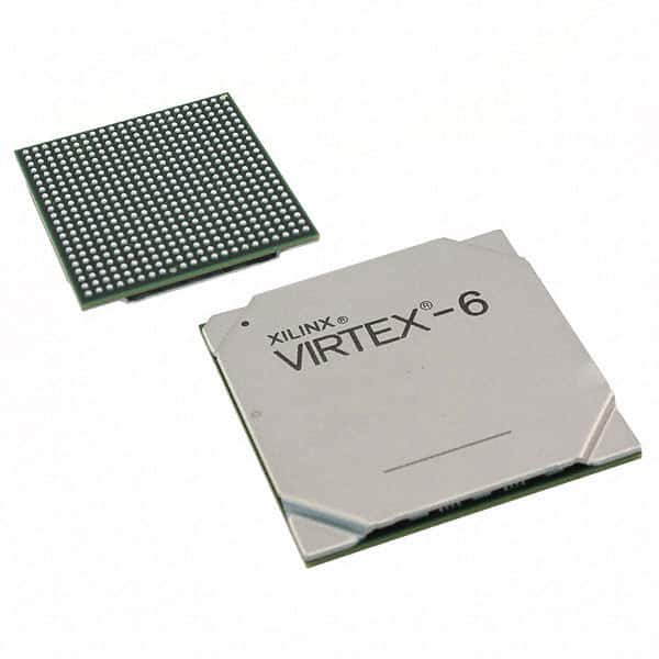
XC6VLX365T-1FFG1759I
Product Overview
Category
The XC6VLX365T-1FFG1759I belongs to the category of Field-Programmable Gate Arrays (FPGAs).
Use
FPGAs are integrated circuits that can be programmed after manufacturing, allowing for flexible and customizable digital logic designs. The XC6VLX365T-1FFG1759I is specifically designed for high-performance applications.
Characteristics
- High-performance FPGA
- Programmable logic cells
- Large number of I/O pins
- High-speed serial transceivers
- Embedded memory blocks
- Flexible clocking options
Package
The XC6VLX365T-1FFG1759I comes in a Flip-Chip Fine-Pitch Ball Grid Array (FFG) package.
Essence
The essence of the XC6VLX365T-1FFG1759I lies in its ability to provide a highly configurable and powerful platform for implementing complex digital designs.
Packaging/Quantity
The XC6VLX365T-1FFG1759I is typically sold individually or in small quantities, depending on the supplier.
Specifications
- Logic Cells: 362,080
- Block RAM: 4,860 Kb
- DSP Slices: 1,920
- Maximum I/O Pins: 900
- Transceivers: Up to 24
- Operating Voltage: 1.0V - 1.2V
- Operating Temperature: -40°C to 100°C
Detailed Pin Configuration
The XC6VLX365T-1FFG1759I has a large number of pins, each serving a specific purpose in the overall functionality of the FPGA. A detailed pin configuration diagram can be found in the product datasheet.
Functional Features
- High-performance processing capabilities
- Configurable logic cells for custom designs
- Flexible I/O options for interfacing with external devices
- High-speed serial transceivers for data communication
- Embedded memory blocks for efficient data storage
- Clocking options to synchronize operations
Advantages and Disadvantages
Advantages
- Flexibility in design implementation
- High-performance processing capabilities
- Large number of I/O pins for versatile connectivity
- Efficient use of embedded memory blocks
- Support for high-speed data communication
Disadvantages
- Steeper learning curve compared to traditional ASICs
- Higher power consumption compared to dedicated hardware solutions
- Limited availability of alternative models with similar specifications
Working Principles
The XC6VLX365T-1FFG1759I operates based on the principles of reconfigurable digital logic. It consists of a matrix of configurable logic cells that can be programmed to implement various digital functions. These logic cells are interconnected through programmable routing resources, allowing for the creation of complex digital circuits.
Detailed Application Field Plans
The XC6VLX365T-1FFG1759I finds applications in various fields, including: - Telecommunications - Data processing and storage - Industrial automation - Aerospace and defense - Medical imaging - Scientific research
Alternative Models
While the XC6VLX365T-1FFG1759I is a highly capable FPGA, there are alternative models available with similar specifications. Some notable alternatives include: - Xilinx Virtex-7 series - Intel Stratix 10 series - Lattice ECP5 series
These alternative models offer similar features and performance, providing designers with options based on their specific requirements.
In conclusion, the XC6VLX365T-1FFG1759I is a high-performance FPGA that offers flexibility, configurability, and powerful processing capabilities. Its wide range of applications and availability of alternative models make it a popular choice among designers in various industries.
Перечислите 10 распространенных вопросов и ответов, связанных с применением XC6VLX365T-1FFG1759I в технических решениях.
Sure! Here are 10 common questions and answers related to the application of XC6VLX365T-1FFG1759I in technical solutions:
Q1: What is XC6VLX365T-1FFG1759I? A1: XC6VLX365T-1FFG1759I is a specific model of Xilinx Virtex-6 FPGA (Field-Programmable Gate Array) that offers high-performance processing capabilities for various technical applications.
Q2: What are the key features of XC6VLX365T-1FFG1759I? A2: Some key features of XC6VLX365T-1FFG1759I include a large number of logic cells, high-speed serial transceivers, embedded memory blocks, DSP slices, and support for various communication protocols.
Q3: What are the typical applications of XC6VLX365T-1FFG1759I? A3: XC6VLX365T-1FFG1759I is commonly used in applications such as telecommunications, aerospace, defense, industrial automation, medical imaging, video processing, and high-performance computing.
Q4: How can XC6VLX365T-1FFG1759I be programmed? A4: XC6VLX365T-1FFG1759I can be programmed using Xilinx's Vivado Design Suite or ISE Design Suite, which provide tools for designing, simulating, synthesizing, and programming FPGAs.
Q5: What is the power consumption of XC6VLX365T-1FFG1759I? A5: The power consumption of XC6VLX365T-1FFG1759I depends on the specific design and operating conditions. It is recommended to refer to the datasheet or use Xilinx's power estimation tools for accurate power consumption calculations.
Q6: Can XC6VLX365T-1FFG1759I be used in safety-critical applications? A6: Yes, XC6VLX365T-1FFG1759I can be used in safety-critical applications. However, it is important to follow industry-specific safety standards and guidelines to ensure the reliability and integrity of the overall system.
Q7: Does XC6VLX365T-1FFG1759I support high-speed serial communication? A7: Yes, XC6VLX365T-1FFG1759I supports high-speed serial communication through its built-in transceivers, which can operate at multi-gigabit per second data rates.
Q8: Can XC6VLX365T-1FFG1759I interface with external memory devices? A8: Yes, XC6VLX365T-1FFG1759I has embedded memory blocks and also supports interfacing with external memory devices such as DDR3 or DDR4 SDRAMs.
Q9: What development boards are available for XC6VLX365T-1FFG1759I? A9: Xilinx offers various development boards that support XC6VLX365T-1FFG1759I, such as the ML605 Evaluation Kit or the KC705 Evaluation Kit, which provide a platform for prototyping and testing designs.
Q10: Are there any known limitations or considerations when using XC6VLX365T-1FFG1759I? A10: Some considerations include managing power consumption, thermal management, signal integrity at high speeds, and ensuring proper design constraints and timing closure for optimal performance. It is recommended to refer to the datasheet and application notes for detailed information on these aspects.
Please note that the answers provided here are general and may vary depending on specific requirements and design considerations.