

Подробную информацию о продукте см. в характеристиках.
XC7V585T-1FFG1157I
Product Overview
Category
The XC7V585T-1FFG1157I belongs to the category of Field-Programmable Gate Arrays (FPGAs).
Use
FPGAs are integrated circuits that can be programmed and reprogrammed to perform various digital functions. The XC7V585T-1FFG1157I is specifically designed for high-performance applications.
Characteristics
- High-performance FPGA with advanced features
- Programmable logic cells for flexible design implementation
- Large capacity for complex designs
- High-speed serial transceivers for data communication
- Integrated memory blocks for efficient data storage
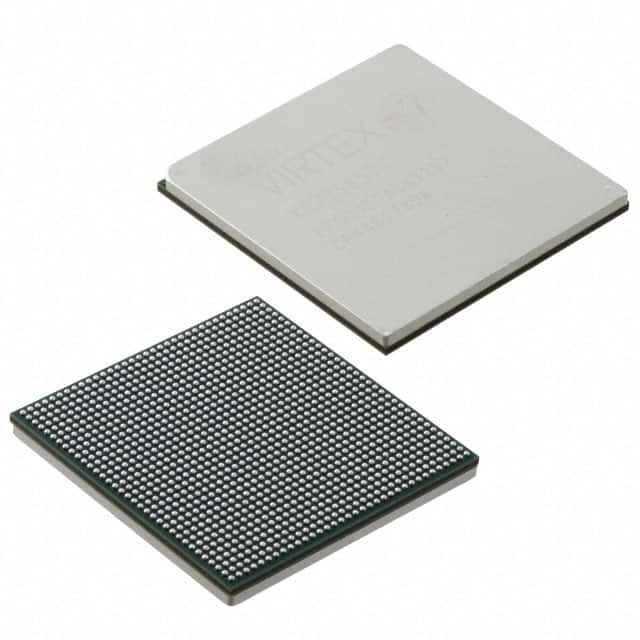
Package
The XC7V585T-1FFG1157I comes in a specific package known as the Flip-Chip Fine-Pitch Ball Grid Array (FFG1157). This package provides excellent thermal performance and reliable electrical connections.
Essence
The essence of the XC7V585T-1FFG1157I lies in its ability to provide a highly configurable and powerful platform for implementing complex digital designs.
Packaging/Quantity
The XC7V585T-1FFG1157I is typically packaged individually and is available in various quantities depending on the manufacturer's specifications.
Specifications
- Logic Cells: 585,000
- Block RAM: 36 Mb
- DSP Slices: 2,880
- Transceivers: 96
- Operating Voltage: 1.0V
- Maximum Frequency: 800 MHz
- Package Type: FFG1157
Detailed Pin Configuration
The XC7V585T-1FFG1157I has a comprehensive pin configuration, which includes input/output pins, power supply pins, clock pins, and configuration pins. For a detailed pin configuration diagram, please refer to the product datasheet.
Functional Features
- High-performance programmable logic cells for flexible design implementation.
- Integrated memory blocks for efficient data storage and retrieval.
- High-speed serial transceivers for fast data communication.
- Advanced clock management resources for precise timing control.
- Built-in digital signal processing (DSP) slices for complex mathematical operations.
Advantages and Disadvantages
Advantages
- High configurability allows for versatile design implementations.
- Large capacity enables the handling of complex designs.
- High-speed transceivers facilitate fast data communication.
- Advanced clock management resources ensure precise timing control.
Disadvantages
- Complexity may require a steep learning curve for inexperienced users.
- Power consumption can be relatively high compared to other devices.
- Cost may be a limiting factor for some applications.
Working Principles
The XC7V585T-1FFG1157I operates based on the principles of reconfigurable computing. It consists of an array of programmable logic cells that can be interconnected to perform various digital functions. The configuration of these cells is determined by the user's design, which is programmed into the FPGA using specialized software tools. Once programmed, the FPGA executes the desired functionality by routing signals through the configured logic cells.
Detailed Application Field Plans
The XC7V585T-1FFG1157I finds applications in various fields, including:
- Telecommunications: Used in high-speed data transmission systems and network infrastructure equipment.
- Aerospace and Defense: Employed in radar systems, avionics, and secure communication systems.
- Industrial Automation: Utilized in control systems, robotics, and machine vision applications.
- Medical Imaging: Applied in advanced medical imaging devices for real-time image processing.
- High-Performance Computing: Used in supercomputers and data centers for parallel processing tasks.
Detailed and Complete Alternative Models
- XC7A200T-1FBG484C: A lower-capacity FPGA suitable for cost-sensitive applications.
- XC7K325T-2FFG900I: A higher-performance FPGA with additional features for demanding applications.
- XC7Z045-2FFG900I: A hybrid FPGA and ARM processor combination for embedded system designs.
These alternative models offer different capabilities and price points to cater to a wide range of application requirements.
In conclusion, the XC7V585T-1FFG1157I is a high-performance FPGA that provides a versatile platform for implementing complex digital designs. Its advanced features, large capacity, and high-speed transceivers make it suitable for various applications in telecommunications, aerospace, industrial automation, medical imaging, and high-performance computing. While it may have a learning curve and higher power consumption, its advantages outweigh the disadvantages for those seeking a powerful and configurable FPGA solution.
Перечислите 10 распространенных вопросов и ответов, связанных с применением XC7V585T-1FFG1157I в технических решениях.
Sure! Here are 10 common questions and answers related to the application of XC7V585T-1FFG1157I in technical solutions:
Q1: What is XC7V585T-1FFG1157I? A1: XC7V585T-1FFG1157I is a specific model of Xilinx Virtex-7 FPGA (Field-Programmable Gate Array) that offers high-performance processing capabilities for various technical applications.
Q2: What are the key features of XC7V585T-1FFG1157I? A2: Some key features of XC7V585T-1FFG1157I include a large number of programmable logic cells, high-speed transceivers, integrated memory blocks, and advanced DSP (Digital Signal Processing) capabilities.
Q3: What are the typical applications of XC7V585T-1FFG1157I? A3: XC7V585T-1FFG1157I is commonly used in applications such as aerospace and defense systems, telecommunications infrastructure, high-performance computing, video processing, and scientific research.
Q4: How can XC7V585T-1FFG1157I be programmed? A4: XC7V585T-1FFG1157I can be programmed using Xilinx's Vivado Design Suite, which provides a comprehensive development environment for designing, simulating, and programming FPGAs.
Q5: What is the power consumption of XC7V585T-1FFG1157I? A5: The power consumption of XC7V585T-1FFG1157I depends on the specific configuration and operating conditions. It is recommended to refer to the datasheet or consult Xilinx's documentation for detailed power consumption information.
Q6: Can XC7V585T-1FFG1157I be used in safety-critical applications? A6: Yes, XC7V585T-1FFG1157I can be used in safety-critical applications. However, it is important to follow industry best practices for designing and verifying the FPGA implementation to ensure reliability and safety.
Q7: Does XC7V585T-1FFG1157I support high-speed serial communication protocols? A7: Yes, XC7V585T-1FFG1157I supports high-speed serial communication protocols such as PCIe (Peripheral Component Interconnect Express), Ethernet, and Serial RapidIO.
Q8: Can XC7V585T-1FFG1157I interface with external memory devices? A8: Yes, XC7V585T-1FFG1157I has integrated memory blocks and supports various memory interfaces such as DDR3, DDR4, and QDR (Quad Data Rate) SRAM.
Q9: What development tools are available for XC7V585T-1FFG1157I? A9: Xilinx provides the Vivado Design Suite, which includes tools for design entry, synthesis, simulation, implementation, and programming of XC7V585T-1FFG1157I.
Q10: Are there any reference designs or application notes available for XC7V585T-1FFG1157I? A10: Yes, Xilinx provides a wide range of reference designs, application notes, and technical documentation to assist users in implementing XC7V585T-1FFG1157I in their specific applications. These resources can be found on Xilinx's website or through their support channels.
Please note that the answers provided here are general and may vary depending on the specific requirements and context of each application. It is always recommended to consult the official documentation and support resources provided by Xilinx for accurate and up-to-date information.