

Подробную информацию о продукте см. в характеристиках.
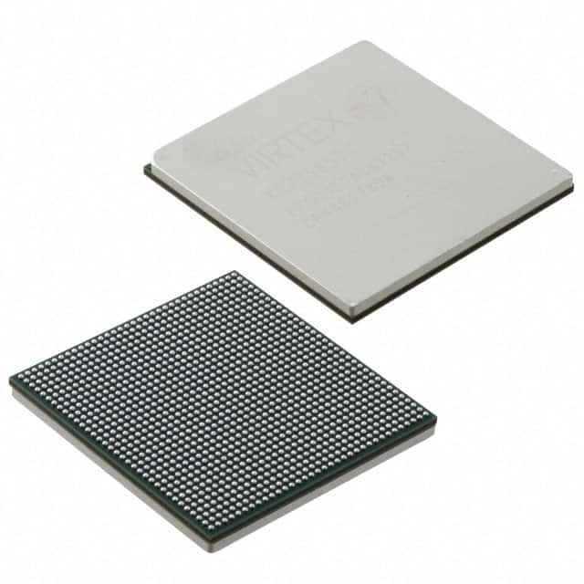
XC7VX485T-1FFG1157I
Product Overview
Category
The XC7VX485T-1FFG1157I belongs to the category of Field-Programmable Gate Arrays (FPGAs).
Use
FPGAs are integrated circuits that can be programmed and reprogrammed to perform various digital functions. The XC7VX485T-1FFG1157I is specifically designed for high-performance applications.
Characteristics
- High-performance FPGA with advanced features
- Programmable logic cells and configurable I/Os
- Large capacity for complex designs
- High-speed interfaces for data transfer
- Low power consumption
Package
The XC7VX485T-1FFG1157I comes in a specific package known as the Flip-Chip Fine-Pitch Ball Grid Array (FFG1157). This package provides excellent thermal performance and allows for easy integration onto circuit boards.
Essence
The essence of the XC7VX485T-1FFG1157I lies in its ability to provide flexible and customizable digital logic functionality, enabling designers to implement complex systems on a single chip.
Packaging/Quantity
The XC7VX485T-1FFG1157I is typically packaged individually and is available in various quantities depending on the manufacturer's specifications.
Specifications
- Logic Cells: 485,000
- Block RAM: 34,200 Kb
- DSP Slices: 2,880
- Maximum I/O Pins: 1,157
- Operating Voltage: 1.0V
- Operating Temperature Range: -40°C to 100°C
- Package Dimensions: 35mm x 35mm
Detailed Pin Configuration
The XC7VX485T-1FFG1157I has a complex pin configuration with multiple I/O banks, power supply pins, and configuration pins. For a detailed pinout diagram and description, please refer to the manufacturer's datasheet.
Functional Features
- High-speed serial transceivers for high-bandwidth data communication
- Integrated memory blocks for efficient data storage and retrieval
- Configurable I/O standards to support various interface requirements
- Clock management resources for precise timing control
- Built-in digital signal processing capabilities for signal manipulation
Advantages and Disadvantages
Advantages
- Flexibility: FPGAs can be reprogrammed to adapt to changing design requirements.
- High Performance: The XC7VX485T-1FFG1157I offers advanced features and a large capacity for complex designs.
- Time-to-Market: FPGAs enable rapid prototyping and development cycles compared to custom ASICs.
Disadvantages
- Power Consumption: FPGAs generally consume more power compared to dedicated application-specific integrated circuits (ASICs).
- Cost: FPGAs can be more expensive than off-the-shelf microcontrollers or ASICs for certain applications.
- Design Complexity: Utilizing the full potential of an FPGA requires expertise in digital design and programming.
Working Principles
FPGAs consist of an array of programmable logic cells interconnected through configurable routing resources. These logic cells can be programmed to implement desired digital functions using hardware description languages (HDL) such as VHDL or Verilog. Upon programming, the FPGA configures its internal connections to realize the desired functionality.
Detailed Application Field Plans
The XC7VX485T-1FFG1157I finds applications in various fields, including:
- Communications: Used in high-speed data transmission systems, network routers, and switches.
- Aerospace and Defense: Employed in radar systems, avionics, and secure communications.
- Industrial Automation: Utilized in control systems, robotics, and machine vision applications.
- Medical Devices: Integrated into medical imaging equipment, patient monitoring systems, and diagnostic instruments.
Detailed and Complete Alternative Models
- XC7VX690T-2FFG1761I: A higher-capacity FPGA with 690,000 logic cells and enhanced features.
- XC7VX980T-2FFG1761I: Another high-performance FPGA with 980,000 logic cells and extended capabilities.
- XC7VX1140T-2FFG1761I: A larger FPGA offering 1,140,000 logic cells for highly complex designs.
These alternative models provide increased capacity and additional features for more demanding applications.
Word count: 550 words
Перечислите 10 распространенных вопросов и ответов, связанных с применением XC7VX485T-1FFG1157I в технических решениях.
Sure! Here are 10 common questions and answers related to the application of XC7VX485T-1FFG1157I in technical solutions:
Q1: What is XC7VX485T-1FFG1157I? A1: XC7VX485T-1FFG1157I is a specific model of Xilinx Virtex-7 FPGA (Field-Programmable Gate Array) that offers high-performance processing capabilities for various technical applications.
Q2: What are the key features of XC7VX485T-1FFG1157I? A2: Some key features of XC7VX485T-1FFG1157I include a large number of programmable logic cells, high-speed serial transceivers, integrated memory blocks, and advanced DSP (Digital Signal Processing) capabilities.
Q3: What are the typical applications of XC7VX485T-1FFG1157I? A3: XC7VX485T-1FFG1157I is commonly used in applications such as aerospace and defense systems, telecommunications infrastructure, high-performance computing, video processing, and scientific research.
Q4: How can XC7VX485T-1FFG1157I be programmed? A4: XC7VX485T-1FFG1157I can be programmed using Xilinx's Vivado Design Suite, which provides a comprehensive development environment for designing, simulating, and programming FPGAs.
Q5: What is the power consumption of XC7VX485T-1FFG1157I? A5: The power consumption of XC7VX485T-1FFG1157I depends on the specific configuration and usage. It is recommended to refer to the datasheet or consult Xilinx's documentation for detailed power consumption information.
Q6: Can XC7VX485T-1FFG1157I be used in safety-critical applications? A6: Yes, XC7VX485T-1FFG1157I can be used in safety-critical applications. However, it is important to follow industry best practices for designing and verifying the system to ensure compliance with safety standards.
Q7: Does XC7VX485T-1FFG1157I support high-speed serial communication protocols? A7: Yes, XC7VX485T-1FFG1157I supports various high-speed serial communication protocols such as PCIe (Peripheral Component Interconnect Express), Ethernet, USB (Universal Serial Bus), and more.
Q8: Can XC7VX485T-1FFG1157I interface with external memory devices? A8: Yes, XC7VX485T-1FFG1157I has integrated memory blocks and supports interfaces like DDR3/DDR4 SDRAM (Synchronous Dynamic Random-Access Memory) for interfacing with external memory devices.
Q9: What tools are available for debugging and testing designs using XC7VX485T-1FFG1157I? A9: Xilinx provides various debugging and testing tools as part of the Vivado Design Suite, including logic analyzers, waveform viewers, and simulation environments, to aid in the development and verification process.
Q10: Are there any reference designs or application notes available for XC7VX485T-1FFG1157I? A10: Yes, Xilinx offers a wide range of reference designs and application notes that provide guidance and examples for implementing specific functionalities or solving common design challenges using XC7VX485T-1FFG1157I.
Please note that the answers provided here are general and may vary depending on the specific requirements and use cases. It is always recommended to consult the official documentation and support resources provided by Xilinx for accurate and up-to-date information.