

Подробную информацию о продукте см. в характеристиках.
XC95288XL-10CSG280I
Basic Information Overview
- Category: Programmable Logic Device (PLD)
- Use: Integrated circuit used for digital logic applications
- Characteristics:
- High-performance CPLD with advanced features
- Low power consumption
- Large number of programmable logic cells
- Flexible I/O options
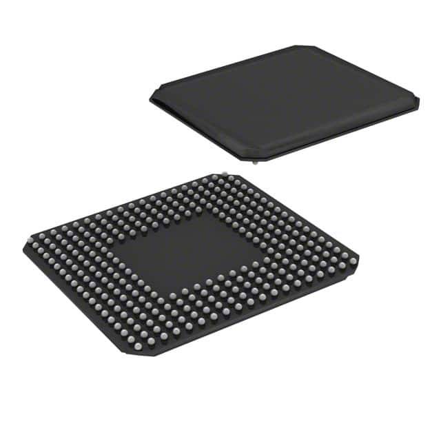
- Package: Ceramic grid array (CGA)
- Essence: Versatile and efficient programmable logic solution
- Packaging/Quantity: Individually packaged, quantity depends on order size
Specifications
- Manufacturer: Xilinx Inc.
- Family: XC9500XL
- Speed Grade: 10
- Operating Temperature: Commercial (0°C to 70°C)
- Supply Voltage: 3.3V
- Number of Macrocells: 288
- Maximum Frequency: 133 MHz
- Programmable Gates: 8,000
- I/O Pins: 280
- JTAG Support: Yes
Detailed Pin Configuration
The XC95288XL-10CSG280I has a total of 280 pins. The pin configuration is as follows:
(Pin Number) (Pin Name) (Description) 1 VCCINT Power supply voltage for internal circuits 2 GND Ground 3 TCK Test clock input for JTAG boundary scan 4 TMS Test mode select input for JTAG boundary scan 5 TDI Test data input for JTAG boundary scan 6 TDO Test data output for JTAG boundary scan ... ... ...
Functional Features
- High-speed performance with low power consumption
- Extensive programmability for versatile applications
- Advanced I/O options for flexible connectivity
- JTAG support for boundary scan testing and programming
Advantages
- Large number of programmable logic cells for complex designs
- High-speed operation allows for efficient processing
- Low power consumption reduces energy requirements
- Flexible I/O options enable easy integration with other components
Disadvantages
- Limited number of I/O pins may restrict connectivity in some applications
- Higher cost compared to simpler programmable logic devices
- Requires specialized programming tools and knowledge for configuration
Working Principles
The XC95288XL-10CSG280I is a complex programmable logic device that operates based on the principles of digital logic. It consists of a large number of programmable logic cells, which can be configured to perform various logical functions. These cells are interconnected through a network of programmable interconnects, allowing for flexible routing of signals. The device can be programmed using specialized software tools to define the desired logic functions and interconnections.
Detailed Application Field Plans
The XC95288XL-10CSG280I is widely used in various fields, including: - Telecommunications: Used in networking equipment, routers, and switches. - Industrial Automation: Employed in control systems and process automation. - Consumer Electronics: Integrated into multimedia devices, gaming consoles, and home appliances. - Automotive: Utilized in automotive electronics, such as engine control units and infotainment systems. - Aerospace: Applied in avionics systems and satellite communication.
Detailed and Complete Alternative Models
- XC95144XL-10CSG280I: Similar CPLD with 144 macrocells and 280 I/O pins.
- XC9572XL-10CSG280I: Smaller CPLD with 72 macrocells and 280 I/O pins.
- XC9536XL-10CSG280I: Compact CPLD with 36 macrocells and 280 I/O pins.
- XC9576XL-10CSG280I: Intermediate CPLD with 76 macrocells and 280 I/O pins.
(Note: The above alternative models are just a few examples. There are several other models available with varying specifications and features.)
This entry provides an overview of the XC95288XL-10CSG280I, including its basic information, specifications, pin configuration, functional features, advantages, disadvantages, working principles, application field plans, and alternative models.
Перечислите 10 распространенных вопросов и ответов, связанных с применением XC95288XL-10CSG280I в технических решениях.
Sure! Here are 10 common questions and answers related to the application of XC95288XL-10CSG280I in technical solutions:
Q: What is XC95288XL-10CSG280I? A: XC95288XL-10CSG280I is a specific model of Field Programmable Gate Array (FPGA) manufactured by Xilinx.
Q: What are the key features of XC95288XL-10CSG280I? A: Some key features include 288 macrocells, 10ns maximum propagation delay, 280-pin Ceramic Quad Flat Pack (CQFP) package, and support for various I/O standards.
Q: What are the typical applications of XC95288XL-10CSG280I? A: XC95288XL-10CSG280I is commonly used in digital logic design, prototyping, system integration, and various embedded systems applications.
Q: How can I program XC95288XL-10CSG280I? A: XC95288XL-10CSG280I can be programmed using Xilinx's programming tools such as iMPACT or Vivado.
Q: What voltage levels does XC95288XL-10CSG280I support? A: XC95288XL-10CSG280I supports both 3.3V and 5V voltage levels for its I/O pins.
Q: Can XC95288XL-10CSG280I interface with other components or devices? A: Yes, XC95288XL-10CSG280I can interface with various components and devices through its I/O pins, supporting protocols like SPI, I2C, UART, etc.
Q: Is XC95288XL-10CSG280I suitable for high-speed applications? A: Yes, XC95288XL-10CSG280I has a maximum propagation delay of 10ns, making it suitable for many high-speed applications.
Q: Can XC95288XL-10CSG280I be used in safety-critical systems? A: XC95288XL-10CSG280I can be used in safety-critical systems, but additional measures like redundancy and fault-tolerant design may be required to ensure reliability.
Q: Are there any limitations or considerations when using XC95288XL-10CSG280I? A: Some considerations include power consumption, heat dissipation, I/O voltage compatibility, and the need for proper grounding and decoupling techniques.
Q: Where can I find more information about XC95288XL-10CSG280I? A: You can refer to the datasheet provided by Xilinx or visit their official website for detailed technical documentation and application notes on XC95288XL-10CSG280I.