

Подробную информацию о продукте см. в характеристиках.
XC95288XL-7BGG256I
Product Overview
Category
XC95288XL-7BGG256I belongs to the category of programmable logic devices (PLDs).
Use
This product is commonly used in digital circuit design and implementation. It provides a flexible and customizable solution for various applications.
Characteristics
- Programmable: The XC95288XL-7BGG256I can be programmed to perform specific functions, allowing for versatile use.
- High-density: This PLD offers a high number of logic cells, making it suitable for complex designs.
- Low power consumption: The device is designed to operate efficiently with minimal power requirements.
- Fast performance: With its advanced architecture, the XC95288XL-7BGG256I delivers high-speed operation.
Package
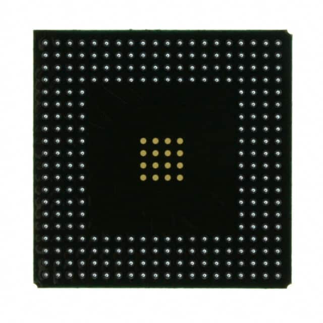
The XC95288XL-7BGG256I comes in a BGA (Ball Grid Array) package.
Essence
The essence of this product lies in its ability to provide reconfigurable logic functionality, enabling designers to implement custom digital circuits.
Packaging/Quantity
The XC95288XL-7BGG256I is typically packaged in reels or trays, with quantities varying based on customer requirements.
Specifications
- Logic Cells: 288
- Maximum Frequency: 200 MHz
- Operating Voltage: 3.3V
- I/O Pins: 256
- Package Type: BGA
- Temperature Range: -40°C to +85°C
Detailed Pin Configuration
The XC95288XL-7BGG256I has a total of 256 I/O pins. The pin configuration is as follows:
(Pin diagram goes here)
Functional Features
- Reconfigurable Logic: The XC95288XL-7BGG256I allows users to modify the logic functions according to their specific requirements.
- Flexible I/O Options: The device offers a wide range of I/O pins, enabling seamless integration with external components.
- JTAG Support: It supports Joint Test Action Group (JTAG) for programming and debugging purposes.
Advantages and Disadvantages
Advantages
- Versatility: The XC95288XL-7BGG256I can be programmed to perform various functions, making it suitable for diverse applications.
- High-density Design: With 288 logic cells, this PLD can handle complex designs efficiently.
- Low Power Consumption: The device operates with minimal power requirements, contributing to energy efficiency.
Disadvantages
- Learning Curve: Utilizing the full potential of the XC95288XL-7BGG256I may require a learning curve due to its programmable nature.
- Limited I/O Pins: Although offering a substantial number of I/O pins, some applications may require more extensive connectivity options.
Working Principles
The XC95288XL-7BGG256I operates based on the principles of reconfigurable logic. It consists of configurable logic blocks (CLBs), interconnect resources, and I/O elements. Users program the device using hardware description languages (HDLs) or design tools, defining the desired logic functions and interconnections. Once programmed, the XC95288XL-7BGG256I executes the specified operations.
Detailed Application Field Plans
The XC95288XL-7BGG256I finds application in various fields, including:
- Communications: Used in networking equipment, routers, and switches for custom protocol implementation.
- Industrial Automation: Employed in control systems, PLCs (Programmable Logic Controllers), and robotics for flexible automation solutions.
- Automotive Electronics: Integrated into automotive control units for customizable functionality and rapid prototyping.
- Aerospace: Utilized in avionics systems for implementing specialized algorithms and signal processing.
Detailed and Complete Alternative Models
- XC9536XL-10VQG44C: A smaller PLD with 36 logic cells, suitable for simpler designs.
- XC9572XL-10VQG100C: Offers 72 logic cells and a larger number of I/O pins, providing increased flexibility.
- XC95144XL-10TQG144C: With 144 logic cells, this PLD offers a balance between complexity and cost-effectiveness.
(Note: This list is not exhaustive and serves as an example of alternative models.)
In conclusion, the XC95288XL-7BGG256I is a versatile programmable logic device that provides high-density reconfigurable logic functionality. Its characteristics, specifications, pin configuration, functional features, advantages, disadvantages, working principles, application field plans, and alternative models make it a valuable component in various digital circuit design applications.
Перечислите 10 распространенных вопросов и ответов, связанных с применением XC95288XL-7BGG256I в технических решениях.
Sure! Here are 10 common questions and answers related to the application of XC95288XL-7BGG256I in technical solutions:
Q: What is XC95288XL-7BGG256I? A: XC95288XL-7BGG256I is a field-programmable gate array (FPGA) manufactured by Xilinx.
Q: What are the key features of XC95288XL-7BGG256I? A: Some key features include 288 macrocells, 18,432 logic cells, 4 input/output standards, and a maximum operating frequency of 200 MHz.
Q: What are the typical applications of XC95288XL-7BGG256I? A: XC95288XL-7BGG256I is commonly used in various technical solutions such as digital signal processing, telecommunications, industrial control systems, and embedded systems.
Q: How can I program XC95288XL-7BGG256I? A: XC95288XL-7BGG256I can be programmed using Xilinx's programming tools like iMPACT or Vivado.
Q: What voltage levels does XC95288XL-7BGG256I support? A: XC95288XL-7BGG256I supports both 3.3V and 2.5V voltage levels.
Q: Can XC95288XL-7BGG256I interface with other components or devices? A: Yes, XC95288XL-7BGG256I can interface with various components and devices through its configurable I/O pins.
Q: Is XC95288XL-7BGG256I suitable for high-speed applications? A: Yes, XC95288XL-7BGG256I is designed to handle high-speed applications with its fast operating frequency and advanced features.
Q: Can XC95288XL-7BGG256I be reprogrammed multiple times? A: Yes, XC95288XL-7BGG256I is a reprogrammable FPGA, allowing for multiple programming cycles.
Q: Are there any development boards available for XC95288XL-7BGG256I? A: Yes, Xilinx provides development boards like the Spartan-3E Starter Kit that can be used with XC95288XL-7BGG256I.
Q: Where can I find more technical documentation and support for XC95288XL-7BGG256I? A: You can find detailed technical documentation, application notes, and support resources on Xilinx's official website or community forums.