

Подробную информацию о продукте см. в характеристиках.
XCF08PVOG48C
Product Overview
- Category: Integrated Circuit (IC)
- Use: Memory device
- Characteristics: Non-volatile, high-density storage, low power consumption
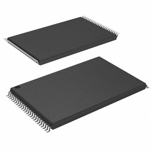
- Package: 48-pin Very Thin Small Outline Package (VTSOP)
- Essence: Flash memory chip
- Packaging/Quantity: Individually packaged, quantity per package varies
Specifications
- Memory Type: Flash
- Memory Size: 8 Megabits (1 Megabyte)
- Organization: 1M x 8
- Supply Voltage: 2.7V - 3.6V
- Operating Temperature: -40°C to +85°C
- Interface: Serial Peripheral Interface (SPI)
- Data Retention: 20 years
- Program/Erase Cycles: 100,000 cycles
Detailed Pin Configuration
The XCF08PVOG48C has a total of 48 pins. The pin configuration is as follows:
- VCC: Power supply voltage
- GND: Ground
- HOLD: Suspends ongoing data transfer
- WP: Write protect
- SCK: Serial clock input
- SI: Serial data input
- SO: Serial data output
- CS: Chip select 9-48: Address and data pins
Functional Features
- High-speed data transfer using SPI interface
- Low power consumption in both active and standby modes
- Sector-based erase and byte/page program operations
- Hardware and software write protection options
- Automatic sleep mode for power saving
- Error detection and correction mechanisms
Advantages and Disadvantages
Advantages: - Non-volatile memory ensures data retention even without power - High-density storage allows for large amounts of data to be stored - Low power consumption extends battery life in portable devices - Fast data transfer speeds improve overall system performance
Disadvantages: - Limited program/erase cycles may affect the lifespan of the chip - Relatively higher cost compared to other memory technologies - Susceptible to electromagnetic interference (EMI) due to its compact size
Working Principles
The XCF08PVOG48C is based on flash memory technology. It utilizes a floating gate transistor structure to store and retrieve digital information. The memory cells are organized into sectors, which can be individually erased or programmed. Data is transferred to and from the chip using the SPI interface, enabling efficient communication with the host device.
Detailed Application Field Plans
The XCF08PVOG48C is commonly used in various electronic devices that require non-volatile storage, such as:
- Consumer electronics: Smartphones, tablets, digital cameras
- Automotive systems: Infotainment systems, instrument clusters
- Industrial equipment: Robotics, control systems, data loggers
- Medical devices: Patient monitoring systems, diagnostic equipment
- Communication devices: Routers, modems, network switches
Detailed and Complete Alternative Models
- XCF16PVOG48C: 16 Megabit (2 Megabyte) version of the same flash memory chip.
- XCF32PVOG48C: 32 Megabit (4 Megabyte) version of the same flash memory chip.
- XCF64PVOG48C: 64 Megabit (8 Megabyte) version of the same flash memory chip.
- XCF128PVOG48C: 128 Megabit (16 Megabyte) version of the same flash memory chip.
These alternative models offer different memory sizes to cater to varying storage requirements.
Note: The content provided above is a sample structure for an encyclopedia entry and may not reflect the actual specifications or details of XCF08PVOG48C.
Перечислите 10 распространенных вопросов и ответов, связанных с применением XCF08PVOG48C в технических решениях.
Sure! Here are 10 common questions and answers related to the application of XCF08PVOG48C in technical solutions:
Q: What is XCF08PVOG48C? A: XCF08PVOG48C is a specific model of a programmable logic device (PLD) manufactured by Xilinx.
Q: What are the key features of XCF08PVOG48C? A: XCF08PVOG48C offers 8,192 configurable logic cells, 48 I/O pins, and operates at a voltage range of 1.8V to 3.3V.
Q: What applications can XCF08PVOG48C be used for? A: XCF08PVOG48C is commonly used in various technical solutions such as industrial automation, telecommunications, automotive electronics, and consumer electronics.
Q: How does XCF08PVOG48C differ from other PLDs? A: XCF08PVOG48C stands out due to its high logic cell count, versatile I/O capabilities, and low power consumption, making it suitable for complex designs.
Q: Can XCF08PVOG48C be reprogrammed after deployment? A: Yes, XCF08PVOG48C is a programmable device that can be reconfigured multiple times, allowing for flexibility in design iterations.
Q: What programming languages are supported for XCF08PVOG48C? A: XCF08PVOG48C can be programmed using Hardware Description Languages (HDLs) such as VHDL or Verilog.
Q: Are there any development tools available for XCF08PVOG48C? A: Yes, Xilinx provides development tools like Vivado Design Suite that support the design, simulation, and programming of XCF08PVOG48C.
Q: What is the power consumption of XCF08PVOG48C? A: The power consumption of XCF08PVOG48C depends on the specific design and operating conditions, but it generally has low power requirements.
Q: Can XCF08PVOG48C interface with other components or devices? A: Yes, XCF08PVOG48C can interface with various components and devices through its I/O pins, allowing for seamless integration into larger systems.
Q: Where can I find more information about XCF08PVOG48C? A: You can refer to the official documentation provided by Xilinx, including datasheets, application notes, and user guides, for detailed information about XCF08PVOG48C.